
AMD is still mid-keynote but that's no reason not to start filling you in on what we know, especially since the CES gang just got a free copy of The Division 2 so we may not see them for a while.
The new Radeon 7 looks similar to the Vega series but offers improved performance, especially at 4K resolutions. According to their internal benchmarks you will see a noticeable improvement from the VEGA series on a number of games.
The new card is not just for gaming, they also showed a slide covering the increases you can expect on a variety of creative software.

As far as the specifications go, we know the card will feature 60 CUs, or 3840 Stream Processors and an impressive 16GB of HBM2 memory with a 1.8GHz GPU at the core. It will require a pair of 8pin PCIe power connectors to drive all of that.

The card will be available on Feb 7th for an MSRP of $699, with a free copy of The Division 2 for as long as supplies last, you can also enjoy that deal on select Ryzen chips That places it under the cost of NVIDIA's top GPUs, but significantly more than the new RTX 2060, but we still have to see where it sits in the benchmark charts!
3rd-Gen Ryzen CPUs Coming
The new third generation Ryzen uses AMD's chiplet design, with a smaller core and a large IO chip. Code-named Matisse, the 7nm Zen 2 desktop parts are not yet ready for release, with final clock speeds not announced. (AnandTech was able to go a little deeper into the the matter before the announcement, and they offer some analysis of the feasability of adding another chiplet to the die and meeting the 16-core number some expected based on the rumors we saw prior to this event. Ed.)

Dr. Su did not share much information of the new chip with us on stage, though we know it may pull less power than a Core i9, at least in Cinebench. Owners of AM4 boards can rest assured knowing that upgrading to the new chips will be as easy as a BIOS update as the socket will indeed remain the same.

Expect more coverage as we catch up!


1.8ghz 16gb hbm2, sign me up.
1.8ghz 16gb hbm2, sign me up. If these cards are able to hit 2 – 2.1ghz under water the performance will not be that far off from a stock 2080ti, food for thought.
It’s only got 60 nCUs enabled
It’s only got 60 nCUs enabled out of 64 so it must be made from a binned/defective Vega 20 die! So how many Shader cores and especially how many ROPs remain after 4 Vega nCUs are disabled. If there are less ROPs because of disabled nCUs then and how does that affect the Pixel Fill Rates on Radeon VII.
A stock 2080ti has 88 ROPs and Vega 10’s max ROP count can never be higher than 64! So if AMD did not up the ROP counts on Vega 20 over Vega 10 and the Vega 20 Die Tapeout is just a 7nm die shrink of the Vega 10 Die Tapeout then 64 ROPs is the maximum for Vega 20 and Radeon VII only uses 60 out of 64 Vega 20 nCUs! Are any ROPs on those disabled nCUs also disabled(?) Radeon VII is going to have a hard time matching the GTX 1080Ti’s Pixel fill rates because that GP102 based Gaming SKUs has 88 ot of GP102’s 96 ROPs enabled.
Most certianly the Power Metrics on TSMC’s 7nm are going to be lower, thermals as well, but the clocks are higher on Raadeon VII! so how much lower(Thermals/Power Usage) will that be with the Radeon VII with the GPU clocked higher.
Nvidia is winning Gaming over AMD with the raw numbers of available ROPs and the higher Pixel Fill rates so unless and until AMD can ge a base Die Tapeout with at least 96 available ROPs AMD’s GPUs are going to be pixel fill rate limited.
AMD did add more DP FP Units to Vega 20 and the ratio is 1/2 DP FP to 1 SP FP and Vega 20 GPU Micro-Arch has some New AI Related ISA exientions that will improve Vega 20’s AI capabilities. So Maaybe some more efficient AI related Upscaling similar to Nvidia DLSS can be done on any Vega 20 based variants like Radeon VII, If, in fact, Radeon VII comes from a binned Vega 20 die!
It seems the 7 nm process
It seems the 7 nm process from TSMC is barely a rebranded 16 nm process… like the 12 nm Fist Fucking Node by nVidia.
It’s not a surprise since most things from Asia are counterfeited. 😀
Really go back to Intel with
Really go back to Intel with your nonsence and tell them to hire better FUDsters than chipman! Really this is high technology and not lowbrow subject matter!
You are obviously some Floyd R Turbo with an axe to grind!
TSMC’s 7nm process has been out for a while so the power/thermal metrics are Known as are the FEOL and BEOL metrics. Intel’s 10nm is late to the party and still not high volume! And according to S/A Intel had to re-engineer the FEOL and the BEOL pitch metrics in order to get that years late 10nm process node out the door. And most of Intel’s shipping 10nm SKUs used in current devces have non working GPU/Graphics beacuse of Intel’s 10nm defect rates, What a process node trainwreck from Intel! That Brian Krasandwitch reaaly borked Intel’s future up before he was removed as CEO!
After all AMD wouldn’t file
After all AMD wouldn’t file for bankruptcy tomorrow if you buy its Radeon Instinct MI50 rebranded as Vega VII… for an outstanding price of 699 USD! :o)
Intel does the same with
Intel does the same with thire CPUs and everbody Bins defective dies into Consumer/Lower variants so nothing wrong with that if Intel does is but AMD is somehow cheating. Just look at Nvidia’s binning operation that gets GTX 1060’s from GP104 DIEs as well as GP106 DIEs.
Your agenda is not very hidden and you may even be Chizow but you are not fooling anyone. AMD stands to bring in more revenues from Epyc Server/HPC sales alone than Nvidia makes from GPUs. Just look at the world wide TAM on Sevrer/HPC CPUs and related sales and that’s many many billions of dollars yearly and growing. AMD getting back to just 23% server CPU market will bring in billions of quarterly revenues without GPU revenues even considered.
What did you smoke man? AMD’s
What did you smoke man? AMD’s server market share is barely ~1 % but speculated to grow fast from the underground.
source:
https://www.theregister.co.uk/2018/08/06/amd_epyc_intel_xeon_x86_server_revenue_share/
That’s an old article and
That’s an old article and AMD’s CEO stated that it will be close to 5% server market share by the end of 2018. 5% by end if 2018 with double digits by end the end of 2019(at least 10% to be in double digits). AMD Lisa Su can not just throw these figures out there as the SEC regulations would not allow for any CEO to state such market share info/projections and not be able to back them up.
Do you know how many hundereds of millions to maybe even single digit billions that 1% of the world wide Server TAM represents. And that’s just the x86 server market because around 96-98% if the world’s servers is still on the x86 ISA at this time.
Look back at AMD’s server market share with just its Opteron CPU offerings on that market at around 23% market share and AMD’s share value was in the $45 randge and AMD’s revenues where much larger on server CPUs at the time because AMD had yet to purchase ATI.
Epyc/Naples(32 ocres/socket) and now Epyc/Rome incoming and AMD moving over to PCIe 4.0 and still offering 128 PCIe lanes and now up to 64 cores per Epyc/Rome socket. AMD’s going to surpass that 23% market share within 2 more years and be earning big bank on Server CPU sales alone. Billions in revenues without even adding in consumer CPU and GPU revenues, or even Professional GPU revenues.
AMD’s Radeon MI60 and MI60’s and Vega 20 based Radeon Pro WX SKUs and Radeon Pro SSD SKUs that also represent even more billions for AMD in addition to AMD’s consumer CPU/GPU revenues! There will even be dual Vega 20 DIEs on single PCIe card variants, just like in the past with AMD’s older generation GPU offerings.
So you need to stop your uneducated foolishness and get a clue!
“AMD Lisa Su can not just
“AMD Lisa Su can not just throw these figures out there as the SEC regulations would not allow for any CEO to state such market share info/projections and not be able to back them up.”
If you can’t backup your words with proofs that’s simply called a L I E !
Nevertheless, that wouldn’t be the first time AMD made false statements… such as Vega 20 not meant for gamers. L O L
Well once AMD’s last quarter
Well once AMD’s last quarter of 2018 SEC filing becomes available we will see and Su can not be too far off from that 5% figure and she’s no dummy like chipman!
Yes CEO’s can not misrepersent any information and Lisa Su stated these figures in a financial analysis phone call where she was quoted:
“AMD has already projected it will achieve a “mid-single digit” share of the server chip market with its current offerings by year-end versus the less than 1% share it had last year. But Su told Barron’s in a phone interview Wednesday the company’s longer-term aspirations are much larger.
When asked if AMD will be able to exceed the historic high of 25% of the server chip market it had in 2006, Su replied, “My vision is to exceed that market share … Yes, AMD’s previous peak was 25% to 26% share, but our current product map is better than the Opteron [the 2006 chip] days.” ” (1)
5 is a mid single digit percentage number that’s actually half way between 1 and 10 and Lisa Su has access to AMD’s actual server CPU unit sales numbers! So there is your year end 2018 projections of around 5% server CPU market share for Epyc/Naples sales alone as Epyc/Rome sales are incoming for the latter half of 2019.
For the server market share projections around the end of 2019 into 2020 time frame that’s double digits by that time frame:
“1. AMD Is Aiming for Double-Digit Server CPU Share in Four to Six Quarters
AMD has set a goal of achieving a mid-single digit server CPU share by the end of 2018, and of eventually having a double-digit share. When I asked about AMD’s time frame for achieving the latter milestone, Su said the exact date will depend on the adoption rate for Rome, which AMD is currently sampling to select clients. However, she also mentioned that AMD considers “somewhere in the next four-to-six quarters” to be a “reasonable expectation” for the company.” (2)
So there you have it and the second refrence(2) of AMD’s double digit server market share time frame. it’s comes with a video of Lisa stating that in 4 to 6 quarters from the date of the article(2) on Nov 8, 2018. So that’s right around the end of 2019 early 2020 time frame give or take a few business quarters from the time of the article, Nov 8 2018, is Lisa Su’s/AMD’s double digit server market share time frame.
The SEC and inverstors will be expecting that AMD’s CEO server market share numbers to be close to what as stated and if thoes figures are too far off then Investors/SEC will want to know why!
So there you have it, for your own googly eyes to see!
(1)
“AMD Chief Lisa Su Aims to Take Massive Market Share From Intel
By Tae Kim Nov. 7, 2018 3:06 p.m. ET ”
https://www.barrons.com/articles/amd-chief-lisa-su-aims-to-take-massive-market-share-from-intel-1541621171
(2)
“AMD CEO Lisa Su Talks to TheStreet: 7 Noteworthy Things She Told Us
Among other things, the chipmaker’s CEO shared details about AMD’s efforts to cater to cloud giants, and was optimistic about the long-term growth outlook for its console processor business.”
By Eric Jhonsa
Updated Nov 8, 2018 8:50 AM EST |Original: Nov 7, 2018″
https://www.thestreet.com/opinion/7-noteworthy-things-amd-ceo-lisa-su-told-thestreet-14772767
Could PCPer and the rest of
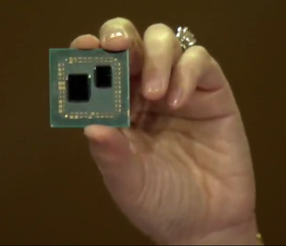
Could PCPer and the rest of the Tech Press grow a pair and start looking for any Informaion on that I/O die on 3rd generation Ryzen/Desktop, like is there any L4 Cache on there on that 14nm I/O die.
That Ryzen 14nm I/O die looks awfully large for just 2 memory chhammels and the other PCIe(4.0 praise deity)/Other controller IP. L4 Cache would be a game changer for gaming workloads and even if some variant came with a GPU Die/Chiplet in addition to a Zen-2 Die/Chiplet!
AnandTech is speculating that there is plent of room for a second Zen-2 chiplet or maybe even a GPU/Graphics chiplet on some other Ryzen 3000/Desktop series variants!
How do you know they are not
How do you know they are not looking? They would be held back b/c of NDA agreements. Anyone could give endless speculating without any basis on reality.
Now, now; you know logic has
Now, now; you know logic has no place in the comments section.
I know about the NDAs but
I know about the NDAs but real Reporters/Tech Press sites purchase their review samples and never consign their Reporters to being neutered by NDAs that limit Freedom of the Press!
That’s why the Online Press is going to pot and the YouTube reporters are doing the actual reporting and fact finding!
That’s Why AdoredTV is so popular with many, he actually works to get at ther truth and is not some extra layer of marketing like some in the Online “Press”!
“real Reporters/Tech Press
“real Reporters/Tech Press sites purchase their review samples and never consign their Reporters to being neutered by NDAs that limit Freedom of the Press…”
WTF are you talking about?
How are the press/reporters supposed to review/talk about new tech if they don’t have access to the tech?
(1) They can’t buy what is not yet for sale.
(2) If they wait for release and buy a real unit, then they will be scooped by “NDA signing hacks” (based on your characterization)
(3) Nothing says that if they wait for release, they will actually be able to get a unit — remember the GPU shortages of recent times where you couldn’t get a unit for love nor money.
NDA’s do not automatically lead to biased reporting.
(1) Biased reviews only hurt the reviewer, no-one will listen to a source if they have been “bitten” by a biased review.
(2) larger/reputable sources are able to get review units because the vendor/manufacturer want details to be made available
(3) NDA’s are a way for the vendor/manufacturer to protect against early performance numbers from being released based on early BIOS/drivers — the AMD presentation showed that drivers can have a significant performance impact (30% based on the last release)
Like GN sometimes does and
Like GN sometimes does and some Websites wait and get theirs from the Retail Channels after release. I do not trust Reviews done under NDA and Before Product release anyways.
I’ll wait for the product to show up Via The Retail channel as I’m no bumpkin that gets fooled by the Snake Oil Salesman/Saleswomen.
The so called “Independent Review Press” appear to be gunning for cushy jobs with Intel, AMD, others anyways if one has been keeping up with Anandtech’s founder ending up at Apple, as well as the Others sites Founders going to AMD and Intel, etc.
NDA directly interfere with
NDA directly interfere with Reporting by limiting the necessary information. NDAs are gag order like and can extend well beyond the introductory timeframe of the review sample in question!
It’s the fear of losing the review samples among the Online Press and losing the page hits and affiliate marketing losses that result from fewer page views. And directly if the NDA is not agreed to the Review sample/samples will not be forthcoming now or maybe in the future also.
This Free Review Sample conflict of interests is the one thing limiting factual discourse and makes the entire online Technology Press suspect. And that will always be the case unless the Review Sample awarding process in taken over by some independent third party and not left in the hands of the CPU/GPU/Other product’s maker hands!
The fix is in and some in the Onlne Technology Press appears rather more interested in obtaining employment from the very same companies whose products that they are supposed to be impartially reviewing.
The YouTube Reviewers like Buildzoid/others that are the LEAST tied in to any free sample/NDA driven or affiliate marketing/direct advertising conflicts of intersets are the only ones that can be more trusted, but still not fully trusted.
It’s The ones with the least strings attatched and readers actually taking the time to read as many reviews as possible and watching Adored TV when he takes an Online Reviewer/Website to task beacause of improper review methodologies that can help get closer to the facts.
The Reviewers are in need of Peer Review of their reviwes now more than ever. So AdoredTV is filling a role there that’s needed and even sometimes GamersNexus/HardOCP will step up also and call other reviewers out. And More of that is needed.
OK PCPer Anandtech’s Ryan
OK PCPer Anandtech’s Ryan Smith has stated that Radeon VII has 128 ROPs and that appears not right at the moment as that would top GP100’s/GP102’s 96 available ROP count.
PCPer needs to sak Ryan Smith if the 128 ROPs count represents the Vega 20 DIE Tapeout’s maximum available complement of ROPs and IS this Radeon VII actually using the full complement of ROP from Vega 20 or not. Because with 128 ROPs the Radeon VII should curb stop the GTX 1080TI with its 88 ROPs or even the Titan XP with a fill GP102 compelment of 96 ROP’s. Something does not add up here with the anandtech article.
From Anandtech:
“Instead, the biggest difference between the two cards is on the memory/ROP backend. Radeon Vega 64 (Vega 10) featured 64 ROPs and 2 HBM2 memory channels running at 1.89Gbps each, for a total of 484GB/sec of memory bandwidth. Radeon VII (Vega 20) doubles this and then some to 128 ROPs and 4 HBM2 memory channels, which also means memory capacity has doubled to 16GB. And then there’s the clockspeed boost on top of this: 1800MHz for the ROPs, and 2.0Gbps for the HBM2 memory. As a result Radeon VII has a lot more pixel pushing power, and a lot more in the way of resources to feed it to get there. Given these changes and AMD’s performance estimates, I think this lends a lot of evidence to the idea that Vega 10 was unbalanced – it needed more ROPs and/or more memory bandwidth to feed it – but that’s something we’ll save for the eventual review.” (1)
Radeon VII has 4 disabled nCUs so that should reduce the available ROP counts for Radeon VII compared to the Vega 20 Base DIE top bin that the Radeon VII is obviously based on. But that ROP count News if true is very big news for raster oriented gaming on Radeon VII based SKUs that come from a binned Vega 20 die! More ROPs mean higher Pixel Fill Rates that directly treanlates into higher FPS metrics.
(1)
”
AMD Reveals Radeon VII: High-End 7nm Vega Video Card Arrives February 7th for $699
by Ryan Smith on January 9, 2019 1:00 PM EST”
https://www.anandtech.com/show/13832/amd-radeon-vii-high-end-7nm-february-7th-for-699
Edit: PCPer needs to sak Ryan
Edit: PCPer needs to sak Ryan Smith
to: PCPer needs to ask Ryan Smith
Damn my proofreading sucks!
Now its back to only 64 ROPs,
Now its back to only 64 ROPs, according to ExtremeTech, its been misreported at 128 ROPs but it’s 64 ROP’s for Radeon VII. And really because of Anandtech/others stating 128 I took that as more likely to be the truth. But AMD/Nvidia have no expectation of anything if they would at least provide the Shader:TUM:ROP numbers when they announce a new consumer gaming GPU variant.
ExtremeTech:
“In this case, there’s a correction we have to issue regarding AMD and its just-announced Radeon VII. Earlier today, ExtremeTech ran a story claiming that this GPU would have a core configuration of 3840:240:128 (GPU cores:texture units:render outputs). This information was based on reporting from other sites who have attended the show and attested to the accuracy of this information. The data was reported in the context of AMD disclosing further details about the GPU while at the show, not as rumor or unverified reporting, which is why we didn’t present the usual caveats when we gave this data.
According to an AMD spokesperson we’ve since spoken to, the number of reported ROPs for the Radeon VII is incorrect. The 128 figure, while widely and credibly stated, is wrong. “Radeon VII is 64 ROPs,” the AMD spokesperson stated to us. The GPU’s actual configuration is therefore 3840:240:64.” (1)
Whitepapers AMD Whitepapers! Are you not a technology company! Intel and Nvidia put out way more whitepaper content!
(1)
“The AMD Radeon VII’s Core Configuration Has Been Misreported”
https://www.extremetech.com/gaming/283649-the-amd-radeon-viis-core-configuration-has-been-misreported
Did she say “699 USD it just
Did she say “699 USD it just works!”? L O L
NIce..
So seeing that it has
NIce..
So seeing that it has only 60 CUs (active), and more transistor counts then Vega64, could indicate that 4 CU’s are disabled.
Then they’ll release Radeon IX with all 64? .. doubt that part, but definitely feels like 4 CU’s are disabled on this silicone.
Still, if I see a preorder, I”m getiing one (at lest) for sure. Need them GPGPU power and at that price, Nvidia can’t compete unless they cut prices a lot. Though there is RTX cores.. so if there will be actual games that support it, AMD will be lagging behind.
Still nice AMD.. NICE
Why do you think they would
Why do you think they would wait until Radeon 9 to unlock all 64? If they don’t release a Radeon 7 SKU with all 64 active then they certainly will with Radeon 8
Anandtech is stating that AMD
Anandtech is stating that AMD doubled the complement of ROPs on Vega 20 to 128 max instead on Vega 10’s 64 ROPs max. [see: anandtech link in other post above for the Quote.}
But depending on the actual number of ROPs on Radeon VII is should beat the GP102 based GTX 1080Ti that has 88 ROPs enabled out of GP102’s full complement of 96 ROPs max!
The GTX 1080TI’s commanding lead in Raster Gaming FPS metrics is directly related to those 88 ROPs and the much higher pixel fill rate(GPixels/s) that the GTX 1080Ti has relative to any other Nvidia/AMD consumer focused gaming GPUs, and even the RTX/Turing SKUs/Variants still have the same ROP counts as the previous generation Pascal variants.
128 ROPs will double Vega 20’s pixel fill rates compered to the Vega 10(Big Die) if both GPUs are running at the same clock rate. Vega 20 runs at higher clock rates than Vega 10 so that’s even higher effective pixel fill rates for any Vega 20 based GPU like the Radeon VII.
Radeon VII is obviously from a binned Vega 20 DIE and some ROPs are going to be disabled as the result of 4 Vega 20 nCU being disabled but still Radeon VII’s ROP counts should top the GTX 1080Ti ROP counts.
This is an interesting development if true!
GPU performance is about a
GPU performance is about a LOT more than just the ROPs. Comparing based on just the ROPs alone is a fools errand.
Also, ROPs are typically tied to memory controller partitions, and usually only get disabled when memory channels are disabled. That is why 1080ti has only 88 of 96 ROPs, it also has a disabled memory channel. I would imagine that the Radeon 7 has all 128 ROPs enabled because AMD does not disable ROPs just because some CU’s are disabled, for example R9 290 has the same amount of ROPs as 290x, as does RX470 and 480 as well as 570 and 580 plus Vega 56 has the same 64 ROPs as Vega 64.
ROPs are where it all comes
ROPs are where it all comes out of and the Higher Pixel fill rates are what results in more frames able to be filled before they are flung out to the monitor.
The GTX 1080TI Had(RTX 2080TI has a little more) at the time the highest Consumer/Gaming GPixel/s fill rates, just refrence TechPowerUP’s GPU database and see the GTX 1080TI’s commanding lead in that GPixel/s fill rate metric.
Nvidia just lowers the quality of its frames so its lomited numbers of Shader cores on Pascal are not overwelmed.
For refrence the Vega 56 has the exact same Numbers of Shader cores and TMUs as the GTX 1080TI but the Vega 56 lacks in the ROP department with only 64, ditto for the GTX 1080(64 ROPs) that’s based on GP104 silicon and not GP102 silicon like the 1080TI. The GTX 1080 TI outperforms the GTX 1080 also and that’s because of those 88 ROPs and that GPixel/s fill rate lead on the 1080TI part.
If the Radeon VII has 128 ROPs then the Titan XP should fall behind in GPixel/s fill rates. Go to TechPowerUP’s GPU database and look and Vega 10(Big Die)/Vega 64 and look at the GPixel/s fill rates and double that plus add in Radeon VII’s faster clocks and that’s even more GPixels/s in fill rate.
Vega 20 must be one hell of a visualization monster and AMD will probably be making a Radeon Pro WX Dual Vega 20 Die variant for the professional markets. The AMD Radeon Pro V340 Datacenter Graphics Card has dual Vega 56(Complement of shader cores/other units) and is a Dual Vega 10 die based Pro SKU. The V340 also has a Hardware ASIC that handles GPU virtualization dubbed by AMD MxGPU Technology. So the V340 will be updated with 7nm Vega 20 based offerings also, and that’s probably what Google and AMD are going to be utilizing for Google’s Project Stream game streaming service.
Right now Raster Gaming still rules with RTX/Ray Tracing going to take time and if the Vega 20 Base Die Tapeout offers 128 ROPs max then for Raster Oriented gaming AMD can now surpass Nvidia’s GPixel/s fill rates by a large margin.
There is also the question of the Vega 20 micro-arch getting 1/2 DP FP to 1 SP FP ratio and Vega 20’s AI related GPU micro-arch ISA extentions that the Vega 10/Vega first generation GPU micro-arch lacks. So if any Radeon VII gets the same feature set as Vega 20 has for the Pro GPU variants then that needs to be looked at also.
Tech Power Up’s database just
Tech Power Up’s database just has theoretical rates, so you could pretty easily calculate what the Vega 20 would be based on ROP count and clock rate.
GP102 has more ROPs than GP104, but also more of everything else, so more is coming in to play than just the ROP count.
A lot of people always thought Fury was very ROP limited, but I don’t. In-fact that’s kind of when the whole bandwagon of AMD cards being ROP limited started IIRC. However, it actually did very well in actual fill-rate tests. For example, see here: https://www.anandtech.com/show/9390/the-amd-radeon-r9-fury-x-review/23 under 3dMark Vantage Pixel Fill. It does very well, beating all but the Titan X. Also note the comments by the Author:
At this point R9 Fury X’s ROPs are pushing more than 40 billion pixels per second, a better than 2x improvement over the R9 290X despite the identical ROP count, and an important reminder of the potential impact of the combination of compression and HBM’s very high memory bandwidth. AMD’s ROPs are reaching efficiency levels simply not attainable before.
Pixel fill rate itself is based on more than just the ROPs. Memory bandwidth and compression also have a big impact on real-world results.
Now, given that Vega 10 has the same amount of compute, texture, ROP’s etc, (however all of it at much higher frequency, so it should scale evenly) as Fury, and that it did not seem to be ROP limited, I don’t think Vega 10 was either. I think the limitation in Fury and Vega 10 was much more due to the performance of the fixed function geometry pipeline, or perhaps some other inefficiency in the architecture.
On another note, I would expect to see the DP FP rate getting limited in the Radeon 7 SKU’s, perhaps down to 1/4 rate (instead of 1/2 FP32), but we will have to see.
“Now, given that Vega 10 has
“Now, given that Vega 10 has the same amount of compute, texture, ROP’s etc, (however all of it at much higher frequency, so it should scale evenly) as Fury, and that it did not seem to be ROP limited, I don’t think Vega 10 was either. I think the limitation in Fury and Vega 10 was much more due to the performance of the fixed function geometry pipeline, or perhaps some other inefficiency in the architecture.
On another note, I would expect to see the DP FP rate getting limited in the Radeon 7 SKU’s, perhaps down to 1/4 rate (instead of 1/2 FP32), but we will have to see.”
Every consumer gaming GPU from AMD and Nvidia at the time not based off that GP102 base die taprout was ROP limited comperd to the GP102 based GTX 1080TI! And the GP102(Pro Market Tapeout) was not intended for the consmer market GP102 was where Nvidia derived mosty Quadro SKUs.
So ROPs and that Pixel fill rate on all GPUs have those theoretical rates and no GPU will achieve the theoretical max 100% of the time but the average GPixel fill rates on the GTX 1080Ti will still be higher as the result of having 88 ROPs. The GP102 based GTX 1080TI has 88 ROPs and will use them whereas the GP104 based GTX 1080 and Vega 10 based Vega 56/64 all have only 64 ROPs and are handily beaten by the 88 ROPs on the 1080Ti in Gaming/FPS metrics.
As far as the DP FP units on the Vega 20 Based Die tapeout based Radeon VII they can not be fine grained disabled and they can still be used for 32 bit calcualtions even if they can not do Packed 32 bit computations. One can perform 32 bit computations on 64 bit FP Units but any results beyond 32 bits accuracy have to be discarded! And that’s no problem because the same happens for any 32 bit FPUs and any computational overflow beyond 32 bits.
So those extra 64 bit FP units can still be useful for 32 bit math operations along with any 32 bit FP units for 32 bit gaming calculations.
Well, if you looked at the
Well, if you looked at the rest of my comment, it proved that Fury was not ROP limited, and by extension Vega wasn’t either. There certainly are limitations in those architectures, but they are not strictly ROP bound.
In any case, there aren’t extra FP64 units, they just use pairs of FP32 units. They can certainly adjust the FP64 rates and have done it in the past. Hawaii had 1/4th speed FP64, but that was only available in the Pro cards like the W9100, where as the R9290/290X was 1/8th speed.
I not disputing ROPs in and
I not disputing ROPs in and of themselves. It’s more that Nvidia’s 5 different Pascal Tapeout’s offered varying amounts of available ROPs compared to that One Vega 10(Big Die) Tapeout that only had 64 ROP max. Nvidia’s GP102 Base DIE tapeout with its maximum of 96 ROPs is what allowed Nvidia that last minute option of taking GP102 and binning out an 88 ROP enabled GTX 1080Ti and retaining the Flagship Gaming GPU crown.
AMD’s Vega 20 Base Die Tapeout has double the number of ROPs for potentially double the pixel fill rates and then some owing to the Vega 20/7nm higher clocks. 64 ROPs in the context of Vega 10 is what I’m mostly concerned with and how that did not compare favorily to Nvidia’s GP102 based GTX 1080Ti on gaming workloads. On compute workloads Vega 10 rivaled even some Quadro/Tesla Pascal variants. Even the GP104 based GTX 1080 at that time had higher clocks and that helped aginst Vega 10 based Vega 64 as both those SKUs had 64 ROPs.
That ONE Vega 10 Base Die Tapeout should have come with at leat 106 ROPs so AMD would have the latitude of creating at least some GPU variant to match GP102’s maximum pixel fill rates. And the reason for 106 is because AMD’s/GF’s 14nm process coud not match TSMC’s higher power lower density process for clock speeds.
Nvidia has made use of lower density libraries with larger cell sizes(More Fins Per Cell) most likely. This is In order to create more 4 fin transistors instead of 3 and 2 fin transistirs that can not be driven to higher clocks than 4 fin based transistors. So those 9.5T and larger libraries can support more 4 fin transistirs compared to 7.5T libraries. Using 9.5T larger libraries with more available fins per cell takes more die space than 7.5T 10 fins per cell libraries but the more 4 fin transistirs the higher the clock speeds so that’s the tradeoff.
So it’s not about Fury’s ROPs it’s about Vega 10’s limited complement of ROPs and the One Vega 10 Base Die tapeout that had insufficient numbers of available ROP to give AMD the same latitude as Nvidia had/has with its 5 different Pascal Base Die tapeouts, GP100, GP102, GP104, GP106/GP108.
Vega 10 should have been designed with excess available ROPs so there could be sufficient variants possible at a later time. The 7nm Vega 20 Base Die tapeout has 128(if Ture) ROPs and that’s going to allow for even more possible Bins that just Radeon VII variant. And there will be Vega 20 dies coming of the difussion lines at TSMC that will have more defects to the point that ther may not be sufficient numbers of working Shader core/nCUs to create MI50’s or Radeon VIIs. And as sure as the sun comes up AMD will be taking those defective/non-performant DIEs and binning out lower performing consumer variants.
GPU/CPU Processor DIEs are also binned on clock speeds and power leakage/usage metrics so the Vega 20 Dies with the most efficient power usage metrics will be used for MI50s and MI60s and any Radeon Pro WX/SSD professional variants that command top dollar. Whereas the Radeon VII(That’s identical to the MI50 in Shaders:TMUs:ROPs) will come from a lessr binned less efficient Vega 20 DIE bin that did not make the power usage/power efficiency grade for professional GPU SKU usage.
AMD’s production on TSMC’s Vega 20 DIE diffusion lines has been ongoing since 2018 and that has resulted in sufficient numders of Vega 20 Die bins that are below the cutoff/binning metrics of Pro GPU usage. That’s resulted in AMD having the option and taking the option of creating the Radeon VII and there will be lower Radeon branded Vega 20 DIE binns also as that’s just the result of the Vega 20 GPU diffusion process and that’s true for any processor production.
What AMD Needs are more GPU Base die Tapeouts that are consumer gaming focused and do not come with any excess shader resources than are needed for Gaming workloads. It’s OK to Bin the Professional GPU variant’s down for Flagship GPU variants as that’s what the GP102 binned to GTX 1080Ti was.
AMD’s also working on Ray Tracing and very likely it’s own Tensor Core IP becaues AMD will need Tensor Core IP for the Professional AI market more than any Ray Tracing IP.
AMD’s semi-custom console Clients are big users of upscaling so you can be damned sure that MS and Sony are wanting some form of AI assisted upscaling IP similar to Nvidia’s DLSS IP. And Sony and MS will probably want Tensor Cores on their next generation Console devices be that baked into the GPU or on the MCM in chiplet from alogside any Zen CPU Die/Chiplets and that GPU Die/Chiplet.
It’s back to 64 ROPs for
It’s back to 64 ROPs for Radeon VII!
It has 128 ROPs. The ROPs
It has 128 ROPs. The ROPs are tied to the memory controllers and the memory controllers were doubled to 4096-bit so the ROPs had to be doubled as well. I think that this is trivial as there are no workloads which will take advantage of 1 TB/s at the moment (the bottlenecks should be elsewhere). I suspect this was done primarily to get the 16 GB of capacity.
No, it was for memory
No, it was for memory bandwidth, mostly for datacenter uses, though. They already do 16GB on Vega FE with the 2048 bit bus.
Not all the HBM2 peak
Not all the HBM2 peak bandwidth maybe but the Pixel Fill Rate on the Radeon VII(Vega 20 DIE Bin) is going to more than double compared to any Vega 10 Die based GPU like the Vega FE that came with 16GB of HBM2 on 2 HBM2 stacks. The Vega FE has the same amount of memory but only half of the effective bandwidth/HBM2 Channels because it’s only using 2 stacks of HBM2 compared to Radeon VII’s 4 stacks of HBM2 and double the number of traces/channels.
Each JEDEC standard HBM2 stack(1024 bits total per stack) is carved up into 8, 128 bit independently operating channels and the HBM2 specifications allow for a each 128 bit channel to be operated in a pseudo 64 bit channel mode.
Radeon VII comes from a binned Vega 20 Die with the same numbers of enabled shader cores as the MI50.
AMD’s MI 60/50 has been in volume production and it’s a known fact for any processor Die production that there will be defective shader cores/other functional blocks on some DIEs. So Radeon VII is AMD making the best of some DIE/Bins that were the result of its Vega 20 based MI 50/60 Vega 20 die production.
Maybe the Radeon VII has some other Vega 20/MI 50/60 features disabled but it’s not been fully disclosed at the moment. I’m very interseted in Vega 20’s xGMI(Infinity Fabric) capabilities and did AMD even enable that xGMI bridge IP on the Radeon VII’s that come from Vega 20 Base DIEs. I’m looking at the photos of the Radeon VII GPU shown at CES and trying to find any better photos that show xGMI ports-PCB Traces/Pins on Radeon VII.
This just proves the point that it’s not the Vega GPU Micro-Arch that was at fault with first gereration Vega. It was really that AMD’s first Vega Micro-Arch based Vega 10 Base die tapeout lacked sufficient numbers of ROPs to properly compete with, at that time, Nvidia’s GP102 Base die tapeout Variant the GTX 1080Ti and its 88 out of GP102’s 96 available ROPs enabled.
So Radeon VII(Vega 20 based) competes in Raster Oriented gaming well compared to the RTX 2080 and Nvidia has really upped the shader core counts of its RTX/Turing Base die tapeouts compared to its eariler GP100, GP102, and GP104/GP106 base die tapeouts.
The RTX 2080: Shading Units: 2944, TMUs: 184(314.6 GTexel/s), ROPs: 64(109.4 GPixel/s), SM Count: 46, Tensor Cores: 368, RT Cores: 46
The Radeon VII: Shading Units: 3840, TMUs: 240(432 GTexel/s), ROPs: 128(230 GPixel/s), Compute Units: 60
So Turing is not lacking for Shader cores compared to Vega 20. TU102 has more Shader coes than full Vega 20 and even the RTX 2080TI has more Shader cores than full Vega 20 this generation. But the Vega 20 based Radeon VII now has 128 ROPs and that Pixel fill rate is going to Double from Vega 10 and then some owing to the higher clocks on Radeon VII.
TU 102: Shading Units: 4608, TMUs: 288, ROPs: 96, Tensor Cores: 576, RT Cores: 72
RTX 2080Ti: Shading Units: 4352, TMUs: 272, ROPs: 88, SM Count: 68, Tensor Cores: 544, RT Cores: 68
Nvidia has more to worry about if AMD doubles up the Vega 20 on a singe PCIe card like AMD did with the dual Vega 10 Die based Radeon Pro V340 with dual Vega/Binned DIEs(similar to Vega 56’s complement of shader cores/TMUs/ROPs for each die) SKU.
It’s not going to be as difficult space wise for AMD to fit 2 Vega 20 dies on a single PCIe card as Vega 20 is smaller than Vega 10. I could see AMD taking some Vega 20 die binns with insufficient numders of working shader cores to even be makde into a Radeon VIIs and maybe doubling up that for some gaming/prosumer variant. But could you just imagine a Dual Radeon VII and the 2 Dies on a single PCIe card using Infinity Fabric-2/xGMI links instead of PCIe links.
According to Wikichip’s Zen 2 entry:
“◾ Infinity Fabric 2
◾ 2.3x transfer rate per link (25 GT/s, up from ~10.6 GT/s)” (1)
So some Dual Vega 20 consumer/prosumer variants may also be offered at some point in time as the Vega 20 Die Bins fill up.
(1)
“Zen 2 – Microarchitectures – AMD”
https://en.wikichip.org/wiki/amd/microarchitectures/zen_2
AMD has Ray Tracing IP in
AMD has Ray Tracing IP in development according to information in this PCWorld article(1)and that extra space on the Ryzen 3000 series SKUs has that definilely has the underlying traces/pads for another CPU die/chiplet!
It’s MOAR COARS for AM4 Folks!
“While rival Nvidia CEO Jensen Huang took a few potshots at AMD’s new Radeon VII GPU, AMD chief executive Lisa Su dropped some bombshells of her own: yes, AMD has its own raytracing GPUs in development, and she hinted strongly that AMD’s 3rd-generation Ryzen chips will launch with more than eight cores.
Su sat down with PCWorld and a few other reporters following her CES keynote address on Wednesday, where she formally launched the 3rd-generation Ryzen and the 7nm “Vega” GPU, known now as the Radeon VII.
Su invited reporters to pepper her with questions, and she responded candidly. The back and forth yielded several pieces of news.” (1)
.
.
.
“More 3rd-generation Ryzen cores
While Su didn’t say for certain that the upcoming 3rd-generation Ryzen would ship with more than the eight cores that she announced on stage, well, it wasn’t hard to read between the lines. “If you look at the evolution of Ryzen, we’ve always had an advantage in core count,” Su said.
In the demonstration showed onstage—comparing a 3rd-generation eight-core, 16-thread Ryzen against an Intel Core i9-9900K, which lost to the Ryzen chip in the Cinebench benchmark—Su said that she wanted to establish a head-to-head comparison, using comparable core counts.
“Some people may have noticed on the package some extra room,” she said with a chuckle. “There is some extra room on that package and I think you might expect we will have more than eight cores.”
AMD has ray tracing GPUs in development, too” (1)
(1)
“AMD’s CEO Lisa Su confirms ray tracing GPU development, hints at more 3rd-gen Ryzen cores”
https://www.pcworld.com/article/3332205/amd/amd-ceo-lisa-su-interview-ryzen-raytracing-radeon.html
I came in with high hope, but
I came in with high hope, but expectations to be disappointed. Well, at least me expectations were surpassed.
At least we know now the
At least we know now the price of the Radeon Instinct MI50. 🙂
Not really becacuse the MI50
Not really becacuse the MI50 may have a lot more of its fabric Error Correcting IP disabled than on the consumer variant/Radeon VII.
Pro GPUs also undergo more expensive Certification/Vetting of Hardware/Firmware/Drivers and those hardwre/software engineers all make 6 figures yearly so that’s not cheap.
Then there are all the makers of the Professional Graphics software packagers that have to certify their software packages on the actual producton Radeon Pro WX SKUs/MI25-50-60 GPU SKUs and that’s more vetting/certification costs for AMD, and Graphics software houses!
Maybe you can estmate the BOM costs on the MI50 but pro grade software/firmware can sometime cost more than the hardware’s cost to develop so Professional GPUs cost more for a reason.
AND may even be eating some of that BOM costs for the hardware because it at least wants to recoup the cost of the Vega 20 DIE production instead of writing off some Binned Vega 20 DIEs that are not performant enough to make the binning grade to be utilised for Pro GPU SKUs.
Pro GPU SKUs cost what they cost becaues of the leveles of QA/QC and software/firmware/hardware certification involved. Professional Drivers take longer to develop and Pro GPUs come with years longer support guarantees with warranties also. Those costs are all amortized into the Total MSRP and figure into the TCO of the end users also.
Is chipman actually a chipmanchild living in chipmama’s basement!
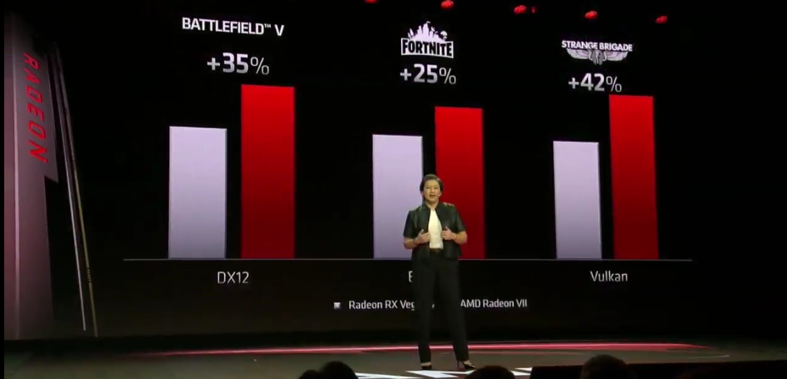
There was also a slide with
There was also a slide with some very selective data displayed. This slide compared Ryzen VII with a 2080 using DX12, DX11 and Vulkan, with 11 and 12 having the same value and Vulkan with a noticeable advantage for AMD.
I have my salt shaker with me.
It looks, but I’ll wait for known reviewers before I get excited.
The demo for a game showing the great frame rates at 4k max settings would have been more impressive if they used a game that people know and can reference.
“with a 2080 using DX12, DX11
“with a 2080 using DX12, DX11 and Vulkan, with 11 and 12 having the same value and Vulkan with a noticeable advantage for AMD”
They are having the same value because they are normalized, that does not mean that they have the same absolut values (that you for some reason think)
Sigh. So much for competition
Sigh. So much for competition bringing value. The 2080 was disappointing because it is too expensive for its level of performance. Stripping out the ray tracing and DLSS for the same stupid price and unimpressive performance doesn’t make this compelling.
Anyone who bought the 1080 Ti nearly two years ago essentially already has this, and they probably spent the same amount on it.
i guess people complain
i guess people complain because they want AMD & Nvidia to release cheaper cards as it’s hard to justify upgrading for so little value.
This card is going to be as fast as a 2080 but cheaper. I guess if we try to 4k game these cards are actually decent.
Next gen games aren’t going to run in 4k rez with any of these cards in as little as 2 yrs from now.
whatever i guess… you have the money and hate nvidia this is the card for you
the xbox keyboard mouse news seems more interesting to get away from all this nonsense and hackers
People complain because they
People complain because they don’t want to overpay for garbages that won’t last more than 3 months by heating like hell!
Chizow that’s definitely you!
Chizow that’s definitely you! Or maybe Chizow is an ESPER of sorts and you have his Hand shoved up your Tuckus! And also you are made of 100% knitted rayon with those googly eyes hot glued on!
What about Vega 20’s support
What about Vega 20’s support for xGMI(Infinity Fabric Based). So the MI60s/50s where displaied with that xGMI bridge and what about that for Radeon VII.
The entire Technology Press is not mentioning Vega 20’s Extended ISA that includes new AI focuesd Instruction extentions(1) on Vega 20 that are not there for Vega 10. Then there are the Larger numbers of DP FP units on Vega 20 for an increased DP to SP FP ratio of 1/2 DP FP to 1 SP FP. Can two 32 bit operation be crammed into one DP FP Unit? What about any AI based upscaling via Vega 20’s New AI instructions extentiosn, or AI based post processing and other AI ralated filtering that may benefit gaming.
Vega 20’s xGMI is AMD’s answer to Nvidia’s NVLink but Nvidia does not fully enable NVLink’s full features on its consumer RTX/Turing SKUs. AMD is more likey to allow for the full xGMI on its cosnumer Vega 20 variants but maybe we will have to wait and see.
I’d love to see 2 Radeon VIIs wired up via xGMI and shareing their VRAM memory in a pooled fashon and using the same memory address space. How will xGMI scale if the Full xGMI(Infinity Fabric) cache coherency protocol is spoken between 2 Radeon VIIs and they act more like a single larger logical GPU with way better scaling than CrossFire.
Vega 20 may just have more Tweaks to other subsystems also so that’s going to be needing some more journalistic digging. Are the drivers that AMD is currently using for Radeon VII the release versions or will there be more driver tweaks incoming for Radeon VII and what about any Fine Wine(TM) expectations for Radeon VII over time. That Fine Wine(TM) for Radeon VII/Vega 20 needs to be looked at in the context of any Fine Wine(TM) that occured with Vega 10. Is Radeon VII/Vega 20 making use Samsung’s Aquabolt HBM2 and what about any memory overclocking potential there, JEDEC has adopted Aguabolt’s metrics into a revised JEDEC HBM2 standard with some other interesting HBM2 tweaks added on top.
These are more questions that need to be asked of AMD before CES is over while the big wigs are all in one place.
Bug the hell out of those AMD Big Wigs and ask them over and over again like the Simpsons Kids in the back seat! What about this and what about that and that other thing!
There are still loads of questions to be answered about Radeon VII/Vega 20.
(1)
“Vega 12/20 Added To AMDGPU LLVM, Confirms New GCN Deep Learning Instructions For Vega 20”
https://www.phoronix.com/scan.php?page=news_item&px=Vega-12-20-AMDGPU-LLVM
How much will price be? It’s
How much will price be? It’s very interesting, as I’m going to purchase a new AMD card.